
Advances in Drawing Process
Traditionally, wire drawing technology has been used to process simple axiasymmetrical goods. The process’s principal drawback is friction at the interface between the drawing tool and the deformed material, which results in variability of characteristics across the drawn wires’ cross-section.
Increasing the product qualities during conventional wire drawing by modifying the die, such as its hardness, surface smoothness, and working zone shape, or changing the processing settings and lubricants, has been studied for many years and appears to have attained technological maturity.
Alternative drawing technologies, such as accumulated angular drawing (AAD) with a non-linear drawing system, ultrasonic vibrations assisted drawing, or ‘‘warm” drawing of barely deformable non-ferrous alloys, have gotten a lot of interest in recent years. Intensive research is also being done to adapt well-known drawing processes to modern steel grades with multi-phase structures (such as AHSS steels), which are becoming more popular due to their improved qualities.
1. Accumulative Angular Drawing (AAD)
The essence of this technology is multi-step drawing using a system of three arched drawing dies with a controlled mutual arrangement of axes.
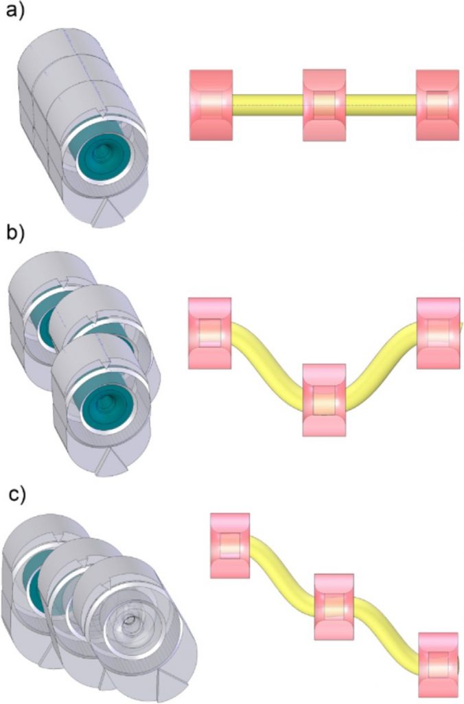
As a result of the drawing process, which can be seen in schematic form in Fig. 1. As the drawn material deforms, a large non-homogeneous accumulation of deformation can be seen. This is a direct result of the bending, twisting, and burnishing that occurs when the material flows through the dies.
The surface layers have the most total equivalent deformation, which is smaller as you get closer to the product’s axis. Because of the non-homogeneity of deformation, the AAD process produces a material with a large nonhomogeneous characteristics distribution at the cross-section. At the same time, high, cumulative plastic deformation energy is present in the material after deformation. As a result, the material annealed after the drawing has a cross-section with a diverse yet very fine grain.
The AAD method can produce a product with high strength and good plastic characteristics when the parameters are properly chosen. The controlled heterogeneity of characteristics, which is a result of the large variation in reinforcement between the surface layers and the layers in the region of the drawn product’s axis, gives the mechanical properties this property.
2. Drawing with longitudinal or circumferential ultrasound vibration of the drawing die
It improves the deformation properties of low-plasticity materials. Piezoelectric or magnetostrictive generators with acoustic power of a few kilowatts are used to generate vibrations with a typical frequency of around 20 kHz. Ultrasound vibration reduces the drawing force, enhances the surface quality, and makes the drawn material more plastic.
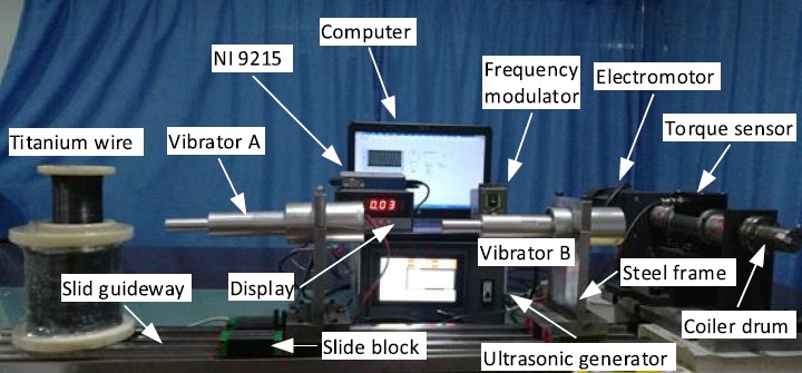
The product is drawn through a die that is axially separated into two parts during the process. Ultrasound vibrations perpendicular to the drawing axis are applied to one die, greatly altering the deformation conditions. Compressive stresses are created in the material by the vibrating die.
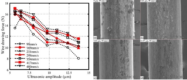
Fig. 3 illustrates an exemplary oscillogram of the force variations when drawing aluminium wire through a split vibrating die as well as a die that does not vibrate perpendicularly. The results of the investigation suggest that using vibration reduces the drawing force significantly. The reduction of the drawing force was within the range of 80 percent depending on the applied elongation and drawing rate.
The effect of drawing force reduction is reduced as elongation and drawing rate are increased. At the same time, the construction of a split drawing die exposes the drawn material to the possibility of flash. It should also be noted that as the drawing force is reduced, the accumulated distortion is reduced, resulting in an increase in plasticity.
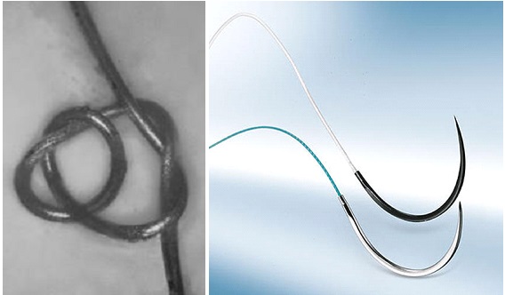
3. Ultra-fine wire drawing for Mg biocompatible alloys for Medical Surgery
画很薄的电线通过激烈的死,process for generating very thin wires from the MgCa 0.8 alloy has been developed. The MgCa 0.8 alloy is one of a class of biocompatible alloys that can be used in medicine, such as surgical sutures. Unfortunately, it has a limited plasticity, making the typical drawing approach hard to generate very thin wires.
A modification of the well-known procedure of warm drawing in a heated die was used to increase the plasticity of the MgCa 0.8 alloy. The use of a heated die allowed wires of the MgCa 0.8 alloy to be produced with a diameter of 0.1 mm. Continuous annealing was added to the process, allowing thin wires with a diameter of 0.05 mm to be produced.
Some of the most promising materials for making soluble surgical threads are magnesium alloys with calcium. Magnesium daily intake is in the range of 375-500 mg per day, while calcium intake is in the range of 800 mg per day. Zinc and iron are two more materials that could be used for surgical sutures.
This metric is 6.5–11 mg for them and 6–20 mg for them, respectively. As a result, magnesium-calcium alloys outperform other materials in terms of allowable body content. These alloys, on the other hand, exhibit low ductility in the cold state and low deformability when drawn.
Hot drawing is used to obtain wire from MgCa0.7 and MgCa0.9 alloys. Furthermore, the drawing process involves distortion of the metal in the heated die and recrystallization as the workpiece moves. These methods enable us to regulate the microstructure of the finished wire and achieve the required ductility.
4. Thermal Drawing of Optoelectronic fibers for optical communications
The creation of high-quality heterojunctions necessitates the close interaction of two distinct semiconductors. Because of the inter-mixing issue, fabricating semiconducting diodes in multimaterial fibres is a significant task.
Although a high-pressure chemical vapour deposition technique with multiple materials deposited sequentially can build a variety of unique devices, including Ohmic junctions, p-n junctions, Schottky junctions, and p-n junctions, the method is not scalable, and the fibre is short.
Prof. Yoel Fink’s group at the Massachusetts Institute of Technology recently developed a novel technology based on the thermal drawing technique for incorporating high-performance commercialized semiconducting diodes into functional fibres. As can be seen in Fig. In step 5a, the prefabricated devices and electrical conductors are first inserted into the polymer-clad preform.
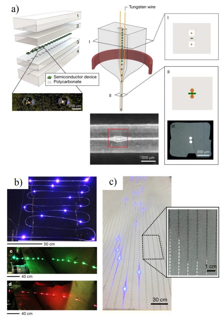
The diodes contained in their pockets flow along the fibre axis as the preform is thermally pulled, and the electrical conductors are continually fed into the fibres. In the neck-down region, the lateral spacing of these conducting wires is gradually reduced until electrical contact with these diodes is achieved.
The authors were able to successfully insert light-emitting and photodetecting p-n diodes into the fibres. Both fibres are woven into a distinct textile polyester fabric on a traditional industrial loom, and they remain fully functional after ten machine wash cycles (Fig. 5b and c).
高速光学发射器和接收器强度grated into fabrics have a wide range of applications. They use two fabrics with receiver-emitter fibres to show a three megahertz bi-directional optical communication link. Diode-based heart rate measurements are also possible. This work establishes a new paradigm for the incorporation of complex functionality into fibres and textiles.
5. Structured fiber drawing with preform wires of Sn-Zn
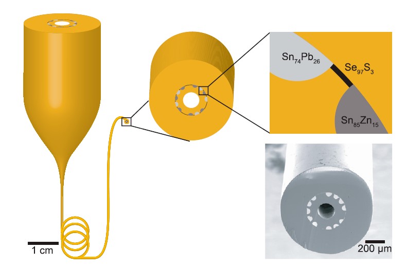
The use of a high-melting-temperature semiconductor in a low-temperature fibre drawing method is demonstrated, extending the range of materials that can be included into fibres significantly. Within a fibre preform, reagents are organised in proximal domains in the solid state.
The preform is fluidized and pulled into fibre at high temperatures, reducing the lateral dimensions and bringing the domains into close proximity to allow chemical reaction. A polymer preform containing a thin layer of selenium contacted by tin–zinc wires is drawn to yield electrically contacted crystalline ZnSe domains of sub-100-nm scales. In the fibre, the in situ produced compound semiconductor serves as the foundation for an electronic heterostructure diode of any length. The capacity to accurately manipulate the geometry and electrical connectivity of materials within fibres at submicron scales opens up new possibilities for expanding the complexity and functionality of fibre systems.
References
- Z. Gronostajski,“Recent development trends in metal forming-a review”, 2019 Elsevier
- Shen Liu,“Experimental Study on Fine Titanium Wire Drawing with Two Ultrasonically Oscillating Dies”,2018 IEEE.
- Andrij Milenina,“The influence of the parameters of hot drawing of MgCa alloys wires on the mechanical properties that determine the applicability of the material as a high strength biodegradable surgical thread”,2020 Elsevier
- Piotr Kustra, Andrij Milenin,“The process of ultra-fine wire drawing for magnesium alloy with the guaranteed restoration of ductility between passes”材料加工技术杂志》,2017年
- Wei Yan,“Thermally drawn advanced functional fibers: New frontier of flexible electronics-a review”,Materials Today, Volume 35, May 2020 Elsevier
- Nicholas D. Orf,“Fiber drawing synthesis”,PNAS 2010